HIFI Diary: A Detailed Science Guide on HIFI Cables – The Digital Signal Cable Edition
Foreword
For a very long time, the HIFI community has been engaged in fierce debates over cables; the argument between “cables matter” and “cables are useless” has raged for decades without a clear winner. In the course of my own reviewing, I have, in fact, wrestled with this dilemma more than once. Yet in the vast majority of cases, I firmly recognize that cables do alter a system’s timbre and improve its overall performance. In what follows, I will attempt to explain the secrets of HIFI cables in the most accessible way possible. This article is very long and may seem rather dry, but I believe it is a truly worthwhile read for any HIFI enthusiast.
Please note that this science guide is presented purely for knowledge sharing. The brands and models mentioned in the text serve only as illustrative examples and do not carry any recommendation. Given the limitations of my knowledge, this text can almost be assumed to be 100% erroneous, so corrections from experienced experts are most welcome. Additionally, I have long been writing HIFI science articles. To read this piece, it is advisable to possess at least a basic understanding of system clocks. I have also previously written several articles analyzing cables:
HIFI Diary: Starting from SATA Data Cables, Discussing the Chaos of DIY Cables – RainLain
HIFI Diary: Selection and Discussion of Ethernet Cables – RainLain
HIFI Diary: A Comparison of Solders – RainLain
HIFI Diary: How USB Cables Affect Sound Quality – RainLain
Main Text
If power cables are the physical interface that supplies energy to the entire system, the role of digital cables is even more subtle and easily misunderstood. In the intuition of many enthusiasts, a digital cable merely transmits “0s” and “1s”—since there are only two states, as long as the cable can convey these two states from the source to the DAC, the job is done, and any remaining effect is dismissed as “metaphysics” or a psychological illusion.
I have pointed out more than once that those who hold this view overlook the real physical form of digital audio signals and grossly underestimate the central role of the clock in digital-to-analog conversion. The scientific basis for why digital cables can audibly and significantly affect sound quality can be summed up in one sentence: The lifeline of digital audio is not the data itself, but the clock (i.e., the clock signal mentioned above); and it is the various properties of the cable that determine the precision of that clock.
1. Analog Waveforms
To understand digital cables, we must first discard the mental inertia that a “digital signal is merely a simple on-off change.” At the physical level, any so-called “digital signal” traveling through a cable is, in essence, an analog voltage waveform varying continuously in time—it is simply assigned the interpretation rule that “above a certain voltage level is 1, below that level is 0.”
Take the S/PDIF coaxial digital signal of CD quality (44.1 kHz sampling rate, 16-bit quantization) as an example. Its raw data rate is 2.8 Mbps (megabits per second), but after biphase mark encoding, the fundamental frequency of the signal actually transmitted on the channel rises to 5.6 MHz. In USB 2.0 High-Speed mode, the data transfer rate reaches 480 Mbps, and its signal fundamental frequency is 240 MHz—this is already a legitimate radio-frequency signal, falling within the VHF band.
Key Point: VHF frequency
[展开/折叠]-
VHF stands for “Very High Frequency,” referring to the band of the radio spectrum with frequencies between 30 MHz (megahertz) and 300 MHz, corresponding to wavelengths from 10 meters down to 1 meter.
The data transfer rate of USB 2.0 is 480 Mbps. On the physical line, data is not directly transmitted at 480 MHz; rather, it uses a 240 MHz clock with double data rate (DDR) sampling—utilizing both the rising and falling edges of the clock—to achieve an effective rate of 480 Mbps. Therefore, the fundamental frequency of a USB 2.0 signal is precisely 240 MHz.
240 MHz falls squarely within the VHF band (30–300 MHz), resting at its very top, right against the lower edge of the UHF band (300 MHz–3 GHz). This is why, when discussing digital audio cables, we refer to USB signals as “RF signals”—in terms of their physical properties, they reside in the same order of magnitude as the transmission frequencies of FM radio broadcasts (88–108 MHz) and VHF television signals.
Recognizing this fact is the cornerstone for understanding all of the following points:
Why is a digital cable no longer just a “connect it and it works” piece of wire?
Because when the signal frequency reaches 240 MHz, the wavelength is as short as approximately 1.25 meters, which begins to be comparable to the physical length of the cable itself (commonly 1–2 meters). At this point, the cable can no longer be treated as an ordinary lumped-parameter circuit; it must be regarded as a distributed-parameter transmission line. Characteristic impedance (such as the 90 Ω specified for USB) starts to play a decisive role, and signal reflections caused by impedance mismatches will tangibly degrade signal integrity.Why is the skin effect so significant?
At a high frequency of 240 MHz, the skin depth in a copper conductor is extremely shallow; current is forced to flow only within a layer a few microns thick at the conductor’s surface. This means the effective resistance of the conductor is far higher than its DC resistance, causing substantial signal loss. This is the exact physical basis for why high-frequency digital cables must employ silver plating or high-purity surface treatments to reduce high-frequency loss.Why is shielding so critical?
A cable 1–2 meters long happens to be a highly efficient transmitting and receiving antenna for a 240 MHz signal. Not only will it radiate energy outward and interfere with other equipment, but it is also extremely susceptible to interference from co-frequency electromagnetic waves in the ambient space (such as walkie-talkies, harmonics of digital TV broadcasts, etc.), directly destroying the eye diagram.Thus, the concept of the VHF band precisely locates what we discuss as “digital signal quality”—from a vague listening impression—into the domain of radio-frequency engineering. It explains why a digital cable transmitting a 240 MHz signal cannot be treated the same as an analog cable transmitting a 20 kHz audio signal.
On a physical line, a digital signal does not appear as an elegant sine wave, but as a voltage pulse train approximating a square wave, with steep rising and falling edges defining the moments of bit boundaries. According to Fourier analysis, an ideal square wave is composed of its fundamental sine wave plus an infinite series of odd-order harmonics. For the receiving end to correctly identify the edge timing of the square wave, the cable must preserve sufficient bandwidth, allowing at least the third, fifth, and even seventh harmonics to pass with low loss. This means: a coaxial cable transmitting a 5.6 MHz SPDIF signal actually needs an effective bandwidth reaching 17 MHz (3rd harmonic), 28 MHz (5th harmonic), and even close to 40 MHz. And a USB 2.0 High-Speed cable needs to handle frequency components well into the gigahertz range.
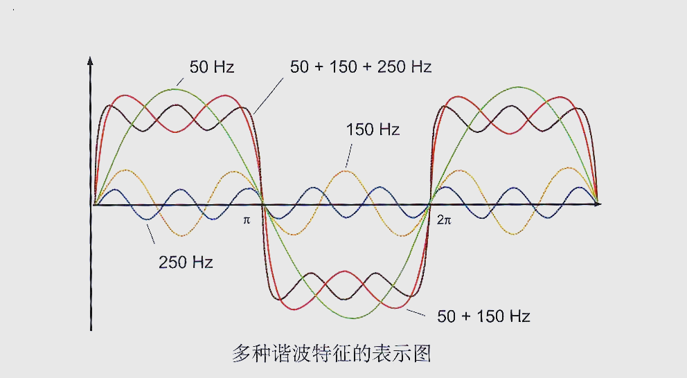
Herein lies the first physical challenge for digital cables: they are radio-frequency transmission lines.
At this order of frequency, no cable is an ideal direct wire anymore; it is a distributed-parameter network—every inch of conductor, every section of dielectric insulation exerts a frequency-dependent influence on the signal in the form of capacitance, inductance, and resistance.
2. Characteristic Impedance
Analog signal cables and power cables focus on the absolute values of resistance, capacitance, and inductance individually, but digital cables enter a stricter conceptual world: characteristic impedance.
Characteristic impedance is not a DC resistance that can be measured with a multimeter. It is a core parameter defined in the context of RF and high-speed digital signal transmission, describing the ratio of the voltage wave to the current wave as a signal propagates along an infinitely long, uniform transmission line (ideally it is a fixed value, but in lossy transmission lines, characteristic impedance is a function of frequency). It is determined by the ratio of the distributed inductance to the distributed capacitance per unit length: Z₀ = √(L/C).
Characteristic impedance is critically important because of an unavoidable physical law: when a signal is sent from a source, conducted through a cable, and finally enters a load, if the characteristic impedances of all three are not consistent, the signal will be reflected at every impedance discontinuity. This is entirely analogous to the partial reflection of light at a glass interface. The reflected wave propagates backward and superimposes on the forward-traveling original signal, causing pulse distortion and overshoot in the time domain, and manifesting as attenuation and notches at specific frequencies in the frequency domain.
For this reason, digital audio interfaces all specify strict nominal characteristic impedances. The S/PDIF coaxial interface standard is 75 ohms, the AES/EBU balanced digital interface standard is 110 ohms, and the characteristic impedance of the USB data lines (the D+/D- differential pair) must be controlled at 90 ohms, with a tolerance of only ±15%. A non-compliant coaxial cable with an intrinsic impedance of, say, 50 ohms (common in RF test equipment), when connected to a 75-ohm S/PDIF input, will have an impedance mismatch as high as 33% ((75-50)/75 ≈ 33%). A large amount of signal energy will be reflected back to the source at the interface, simultaneously wasting signal budget and causing a drastic degradation in waveform quality.
Strict control of characteristic impedance permeates every structural detail of the cable. It demands precise mathematical coordination among conductor diameter, conductor spacing, insulation material, and the dielectric constant of the plugs. This is the fundamental reason why high-quality digital cables are extremely fastidious about conductor geometry precision and insulation material choice—it is not some arcane tuning, but a basic requirement of RF engineering for physical consistency.
3. From Square Wave Degradation to Clock Jitter
Now we arrive at the central dilemma of digital audio: jitter. A fact that has been repeatedly validated is that differences in digital audio sound quality very rarely originate from bit errors themselves. Modern digital audio protocols typically possess some degree of error correction capability, but consumer-level protocols like SPDIF and UAC (USB Audio Class) employ only very simple parity checks and lack forward error correction with retransmission. More critically, even under zero bit-error conditions, the quality of the clock recovered by the SPDIF receiver from the signal can vary enormously depending on the cable’s properties (which is why clock synchronization becomes especially necessary).
To understand this mechanism, we must start with the clock architecture of a DAC. In the vast majority of digital audio systems, the decoder either extracts the clock from the incoming digital signal using a phase-locked loop (PLL), or uses a local precision clock and synchronizes the source clock via a PLL. Whichever scheme is used (except for UAC asynchronous mode), the ultimate clock fed to the D/A conversion chip derives its purity to a high degree from the waveform quality of the original digital signal.
The core manifestation of a degraded waveform is the rounding of the square wave edges. When cable bandwidth is insufficient or impedance is severely mismatched, the supposed steep rising and falling edges become slow and slanted. For the receiver, determining “when the level transition occurred” requires setting a threshold voltage. Once the signal edge is no longer an instantaneous jump but a sloping ramp, tiny noise superimposed on the line will be translated into a significant shift in the instant the threshold is crossed. The magnitude of this shift is measured in picoseconds, but as we have discussed previously, even just 1 nanosecond of jitter on a 44.1 kHz clock can already equate to the error of the least significant bit in 16-bit audio.
Key Point: The Dilemma of USB
[展开/折叠]As mentioned, the great advance of USB Asynchronous mode is that it lets the DAC’s own femtosecond crystal oscillator dominate the clock, essentially eliminating the clock jitter transmitted from the PC. However, it introduces a side effect not present in SPDIF: a USB cable contains both data and power lines simultaneously. SPDIF/AES are susceptible to jitter, so the source clock is very important. USB, on the other hand, is very prone to conducting noise from the source (such as a PC) directly into the DAC. Even when engineers make substantial efforts to isolate it, USB outputs are still typically “noisier” than SPDIF or AES.
This noise introduced via USB is what we call common-mode noise. USB’s common-mode noise originates from its original design philosophy, because USB transmission requires a GND line as a voltage reference, yet that very same wire also serves as a galvanic connection path between the computer and the DAC. As a reference, it cannot be broken (otherwise USB will not transmit data). But as a galvanic connection, it becomes precisely the low-impedance pathway through which noise inside the computer floods into the DAC. Thus, the GND dilemma in USB audio is a consequence of the USB standard prioritizing cost and data-transport universality at the time of its creation, without making compromises for the electromagnetic compatibility requirements of high-fidelity audio.
The skin effect and dielectric loss are two fundamental physical processes that cause the rounding of the square wave. The skin effect forces the high-frequency components (the odd harmonics required for the square wave’s steep edges) to conduct only within an extremely thin skin at the conductor’s surface, making the effective resistance for these high-frequency harmonics far greater than the DC resistance, resulting in the selective attenuation of high-frequency components.
Key Point: Skin Effect
[展开/折叠]3.1 A Reluctant Necessity
First, let us clear up a common misconception: the high-frequency signal itself does not have any consciousness to actively choose to travel on the conductor surface. It is “forced” to the surface by the reverse eddy currents induced electromagnetically within the conductor—a passive physical consequence.When alternating current flows through a conductor, the current itself generates an alternating magnetic field around the conductor. This alternating magnetic field penetrates the conductor itself and, in turn, induces eddy currents. According to Lenz’s Law, the direction of the induced eddy currents always tends to oppose the change in the original current that created them. At the center of the conductor, the eddy current flows opposite to the original current; the two sum, resulting in the net current being maximally weakened. The closer to the surface, the fewer the magnetic field lines, the weaker the eddy current, and the smaller the net current loss. The final result is this: the vast majority of the current concentrates and flows within an extremely thin annular region close to the surface; moving toward the center of the conductor, the current density drops lower and lower, to the point where it can be virtually nonexistent.
Therefore, the primary effect of the skin effect is a dramatic reduction in the effective conduction cross-section for high-frequency signals, which leads to an increase in the effective high-frequency resistance and the consequent attenuation, rather than making high frequencies travel faster.
3.2 Skin Depth
To quantify this effect, engineers defined a parameter called skin depth (δ), which refers to the thickness of the layer at which the current density has decayed to about 37% of its value at the surface. The formula is δ = √(2ρ / ωμ), where ρ is resistivity, ω is angular frequency, and μ is magnetic permeability.Taking a copper conductor as an example (resistivity 1.72×10⁻⁸ Ω·m, relative permeability ≈1), the skin depth varies with frequency roughly as follows:
At 60 Hz (mains power): the skin depth is about 8.5 mm. The radius of common household power cables falls within this value; the skin effect has virtually no impact, and current flows uniformly across the entire cross-section.
At 1 kHz (audio midrange): the skin depth is about 2.1 mm. The core radius of most audio cables is still smaller than this, and the impact remains limited.
At 5.6 MHz (S/PDIF fundamental frequency): the skin depth plummets to only about 28 microns, thinner than ordinary office paper.
At 240 MHz (USB 2.0 fundamental frequency): the skin depth is less than 5 microns, on the order of one-tenth the diameter of a human hair.
This is the physical reality for digital cables: signals with fundamental frequencies from several megahertz up to hundreds of megahertz are forced to conduct only within a skin layer a few microns thick at the conductor surface. The vast bulk of the copper inside the conductor is merely ornamental, contributing nothing to signal transmission.
3.3 Impact on Digital Cables: The Blade Edge of the Square Wave is Blunted
The skin effect directly causes the high-frequency AC resistance to be vastly larger than the DC resistance. A thick copper wire with extremely low DC resistance, when subjected to megahertz frequencies, sees its effective conducting cross-section squeezed into an extremely thin outer layer, and its actual resistance can skyrocket by tens or even hundreds of times. This elevated resistance selectively attenuates the signal’s high-frequency components—namely, those odd harmonics that constitute the steep edges of a square wave. With the harmonics weakened, the originally sharp square-wave edges become slowly sloping. This is precisely one of the fundamental physical mechanisms behind “eye width” narrowing, “eye height” collapse, and the worsening of jitter.3.4 The Engineer’s Solutions: Silver Plating and Litz Wire
To combat the skin effect, audio cable engineering has two classic solution paths.The first is silver plating. By plating the conductor surface with a layer of high-conductivity pure silver, utilizing silver’s status as the metal with the highest electrical conductivity, a lower-loss path is provided for the high-frequency current forced to travel on the skin. This is why mid-to-high-end digital cables often feature “silver-plated copper” conductors—the true engineering value lies in the high-frequency overtone region, not in DC performance.
The second is the Litz structure. A single thick conductor is replaced by multiple strands of extremely fine, individually insulated wires twisted together. Each fine strand presents an independent surface layer to the high-frequency signal, and the total surface area of the multistrand bundle is far greater than that of a single thick conductor. This equivalently provides more “skin” for the high-frequency current to flow through, substantially offsetting the AC resistance increase caused by the skin effect. Litz wire is also commonly used in high-frequency power cables and speaker cables, but its effectiveness is significantly pronounced only when the electromagnetic wavelength is below roughly 50 kHz–2 MHz; for digital signal transmission in the tens to hundreds of megahertz range, Litz wire’s effectiveness drops considerably, and one must turn to silver-plated conductors and strict characteristic impedance control.
At the same time, the dielectric loss factor of the insulation material directly absorbs high-frequency signal energy, converting it into heat, and further exacerbates the destruction of the rising edge. A well-designed digital cable must be doubly optimized in both conductor surface treatment (such as silver plating to leverage the high-conductivity surface layer of silver) and the selection of low-loss dielectric (such as foamed polyethylene FPE or air-filled structures, replacing solid PVC), to maximize the retention of the amplitude and phase relationships of the harmonics that form the square wave edges.
4. The Eye Diagram
All of the above discussions regarding impedance, bandwidth, and loss ultimately converge on a single test instrument—the eye diagram. The eye diagram is the universally recognized benchmark for measuring the physical quality of a digital signal. Using an oscilloscope’s persistence mode, it superimposes tens of thousands of random data pulses onto the same screen. If the signal quality is perfect, the rising edges, falling edges, high levels, and low levels of all pulses will overlap precisely, opening up a clearly defined, vertically symmetrical “eye” shape in the center of the screen.
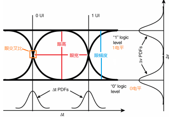
The eye diagram provides three key criteria. Eye height represents the effective signal-to-noise ratio margin—the larger the eye height, the greater the amplitude noise must have before it can cause a bit decision error. Eye width represents the effective decision timing window—the wider the eye width, the larger the time tolerance within which the receiver can accurately sample, directly reflecting the system’s ability to resist jitter. The slope of the edges is directly related to jitter—the steeper the edges, the smaller the threshold-crossing time deviation caused by the same noise amplitude.
An excellent 75-ohm coaxial digital cable, even after transmission over several meters, can still display a clear, wide-open, sharp-edged eye diagram on an oscilloscope. Conversely, a poorly designed cable, even if shorter in length, may present a fatigued eye diagram with collapsed eye height, narrowed eye width, and blurred edges—this is the direct physical manifestation of high jitter. The eye diagram cares nothing about musical content or brand premium; it only cares about one thing: whether this cable can, at the electrical layer, deliver the original timing information intact and losslessly to its destination.
5. Shielding of Digital Cables
The shielding requirements for digital cables are far more stringent than those for power cables or analog cables, stemming from two overlapping factors. First, the signal transmitted by the digital cable itself is already in the megahertz to gigahertz RF bands, meaning that electromagnetic interference from the same frequency bands in the external environment can cause direct in-band contamination of the signal—this is not an audio-domain concept of “external noise superimposed on the audio signal,” but an RF-domain concept of “RF interference directly confusing the receiver circuit’s judgment of signal edges.” Second, the digital cable can simultaneously act as an RF transmitting antenna, radiating its internal clock and data pulses outward and contaminating other, more sensitive analog stages in the system.
In constructing the shielding structure, digital cables follow a clearly tiered engineering rule. The most basic coaxial cable employs a composite structure of a single-layer braided copper shield plus aluminum foil, with coverage exceeding 95%. More comprehensive designs add an extra layer or even multiple independent shield layers, attenuating the interference energy stage by stage.
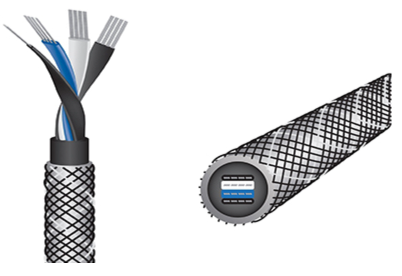
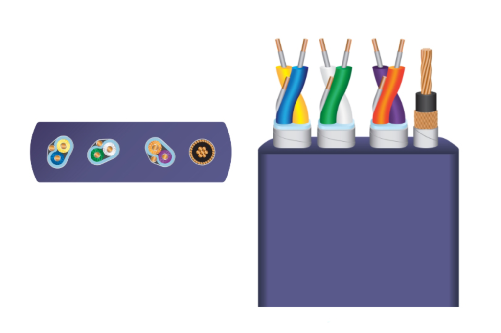
The structural challenges faced by USB digital cables are even more formidable than those of coaxial cables. Inside a standard USB cable, the high-speed data differential pair (D+ and D-) is routed in parallel and tightly bundled together with the 5V power line and the ground line. When connecting a DAC or interface that is USB-powered, the load current on the power line—especially dynamic current modulated by the changing operation of the DAC chip—generates a varying electromagnetic field around the data lines, directly interfering with the signal pair through near-field coupling. This is exactly the engineering reason why many high-end USB interfaces use external linear power supplies for independent power delivery, and why audiophile USB cables strictly isolate the data channel from the power channel internally, implementing split-body shielding.

You May Also Like
HIFI Diary: A Detailed Science Guide on HIFI Cables – The Analog Cable Edition

HIFI Diary: How to Judge/Describe Sound Quality? A Detailed Explanation of Hi-Fi Testing Dimensions